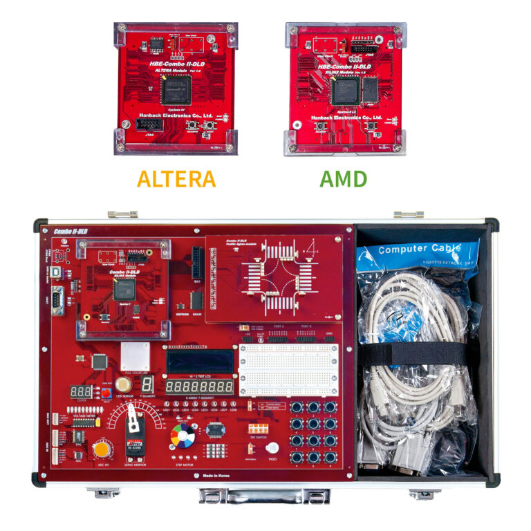
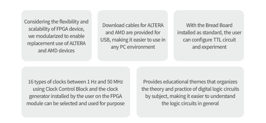
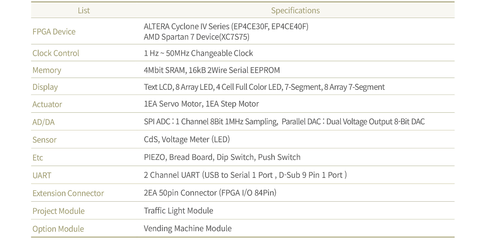
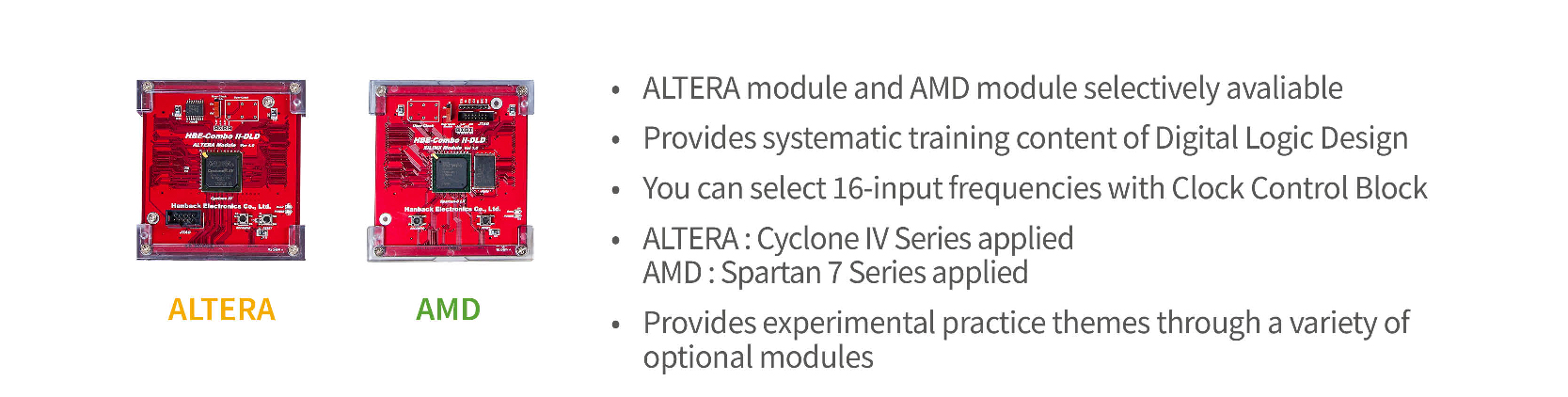
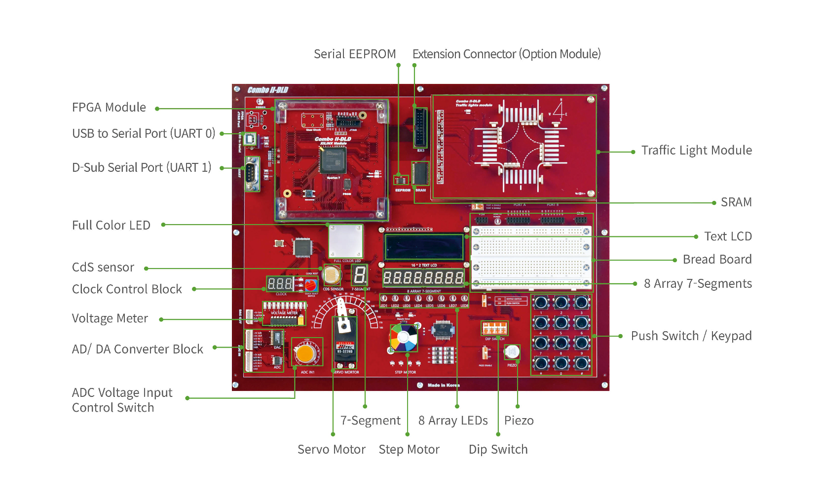
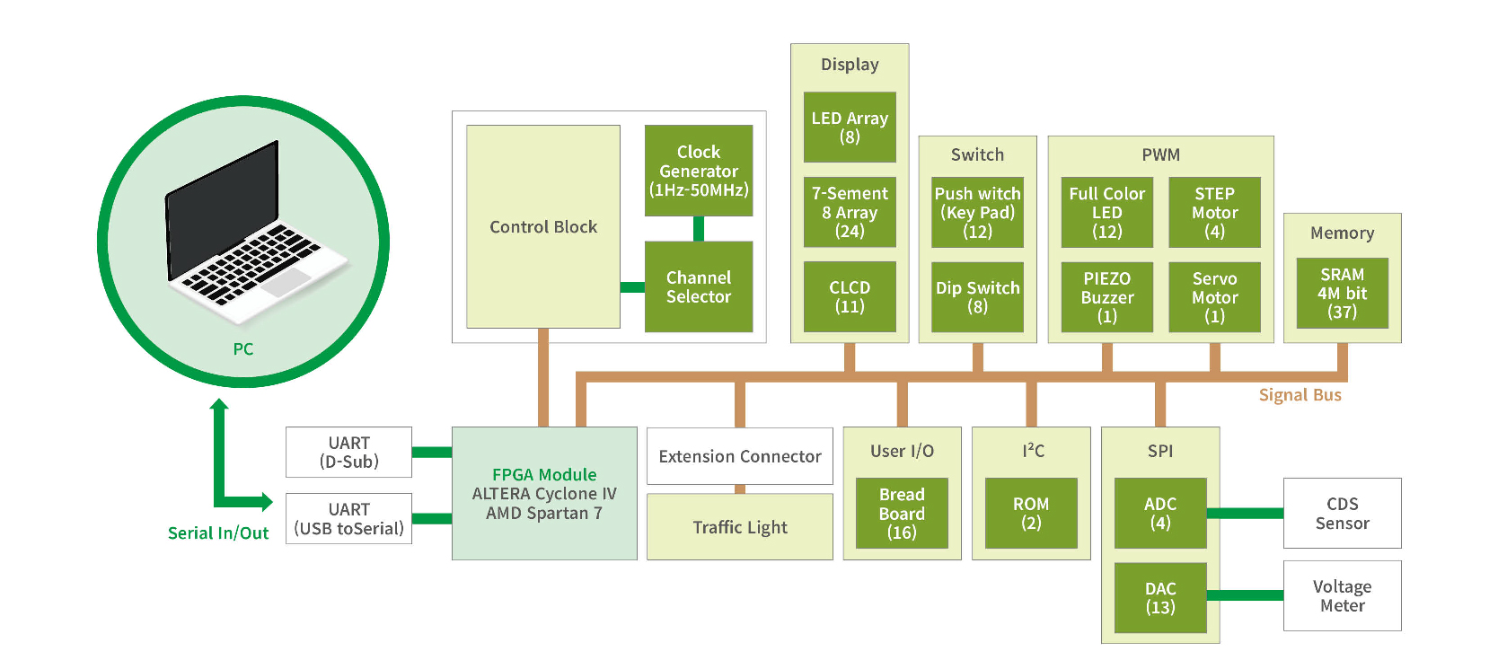
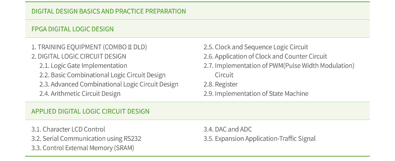
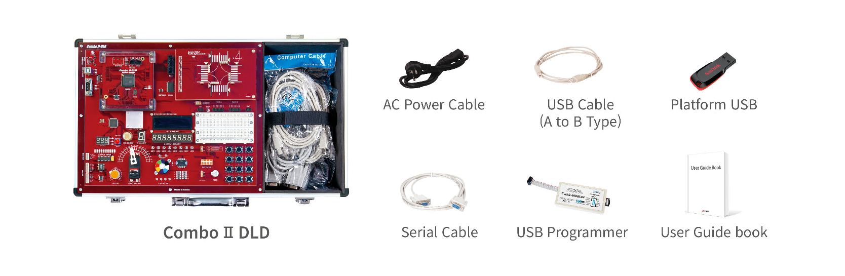
HBE-Combo II DLD (Altera, Xilinx)

FPGA Digital Circuit Design Trainer based ALTERA/XILINX

  • Available to select ALTERA and XILINX(extra option) FPGA module
  • Systematic Digital Logic Design Education Theme Supply 16 kinds of Input Frequencies through Clock Control Block
  • Use of The latest FPGA (ALTERA – Cyclone IV Series, XILINX – Spartan 6 Series) Device
  • Various Experiment Themes using Various Option Modules (Fully compatible HBE-Combo II option module

Features

  • Modular design considering Flexibility and Expansibility of FPGA device enable to select ALTERA and XILINX device.
  • Provides Education Theme organized by subjects of digital logic circuit theory and experiment procedure in order to understand the logic circuit easily.
  • User can select the clock from user’s Clock Generator which mounted at FPGA module or choose 16types of internal clock(1Hz~50MHz) from built-in Clock Control Block.
  • It is fully compatible with HBE-Combo II option modules so user can use previous FPGA application theme without change.
  • User can make and test of user’s TTL circuit using built-in Bread Board as default.
  • User download program to FPGA easily using supplied USB download cable.

Design Environment

ALTERA : Quartus II Web Edition
XILINX : ISE Webpack Design Software

Design software is available to download
free of charge from each device homepage
(Altera/Xilinx).

Configuration and Names

Block Diagram

Hardware Specifications

Option Modules

Training Contents

Designing Digital Logic Circuit with HBE-Combo II-DLD

1. Introduction to Digital Logic Circuit(Fundamental Logic Gate Experiment)
2. Combinational Logic Circuit Experiment 1(Adder, Encoder and Decoder and 7 Segment
Decoder Design)
3. Combinational Logic Circuit Experiment 2 (Multiplexer and Demultiplexer, Comparator and
Code Converter)
4. Sequential Logic Circuit Experiment 1(Clock, Flip-Flop and Latch)
5. Sequential Logic Circuit Experiment 2(Register Design)
6. Counter Experiment 1(Asynchronous Counter and Synchronous Counter)
7. Counter Experiment 2(Clock Divider Circuit and Clock Design with Counter)
8. PWM control Experiment (Full Color LED and Servo Motor control with PWM)
9. Parallel Interface Experiment (SRAM control and Text LCD control)
10. Serial Interface Experiment (I2C Interface Design and SPI Interface Design)
11. State Machine Experiment 1(Moore machine and Mealy machine)
12. Design Project Experiment 1(8 Array 7-Segment output Stop Watch Design)

Components